-
Robot
Most Wanted

- Rep Power
- 82
 Leaker Believes Samsung Exynos 2600 Mobile Chip Will Feature AMD "JUNO
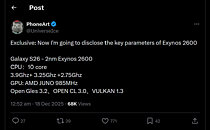
Earlier in the month, Samsung's marketing team initiated their Exynos 2600 promotional campaign. At the time, official teaser material did not provide any substantial hints about the next-gen mobile chipset's technical underpinnings. Weeks later, a fresh leak has laid out the cutting-edge mobile processor's fundamentals. PhoneArt's social media post seems to confirm previous predictions about an overall 10-core design, and being based on an important in-house 2 nm node process. Today's prediction did not outline the Exynos 2600 SoC's cluster configuration, but previous outpourings have settled on a "1x Prime + 3x Performance + 6x Efficiency" internal setup. PhoneArt reckons that the prime core will reach a maximum clock frequency of 3.9 GHz. A commenter, Erencan Yılmaz, reckons that this figure should be reduced to 3.8 GHz, due to power consumption considerations when looking at a 2 nm GAA-based design.
Supposedly, max. performance core speed is 3.25 GHz, while efficiency-oriented units can only reach up to 2.75 GHz. In the past Samsung and AMD have co-developed various Xclipse integrated graphics solutions, for proprietary smartphone platforms. Industry observers expected this RDNA-based collaboration to continue into a new generation. The fresh mentioning of a mysterious "AMD JUNO" iGPU has caused some confusion—this new Team Red IP is said to be clocked at 985 MHz. Additionally, PhoneArt claims that "JUNO" supports modern APIs: OpenGL ES 3.2, OpenCL 3.0, and Vulkan 1.3. It is plausible that "JUNO" could be a codename for the speculated "Xclipse 960" integrated graphics processor.

More...
 Posting Permissions
- You may not post new threads
- You may not post replies
- You may not post attachments
- You may not edit your posts
-
Forum Rules


