-
Robot
Most Wanted

- Rep Power
- 82
 TSMC Prepares CoWoS to CoPoS Shift with 750 × 620 mm Panels
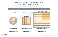
TSMC is reportedly preparing to transition its advanced packaging strategy from CoWoS to a panelized approach called CoPoS, which stands for Chip-on-Panel-on-Substrate. The company plans pilot lines as soon as 2026 and aims for mass production between late 2028 and the first half of 2029. The change involves swapping around 300 mm silicon interposers for large square and rectangular panels, with early formats measuring around 310 × 310 mm and later options extending to 515 × 510 mm and even 750 × 620 mm. That larger, square format is intended to reduce wasted edge area, allow bigger reticles and masks for AI accelerators, and make it easier to place more dies and HBM on a single package.
Technically, CoPoS combines CoWoS ideas with fan-out panel-level packaging, building RDL layers on glass or sapphire panels rather than on circular silicon. TSMC is lining up CoPoS development and production at its AP7 Chiayi campus, where phases 4 and 5 are expected to host panel work, and it plans related capacity in future Arizona facilities. Equipment and tooling orders are already being placed, and the supplier list includes global names like KLA and Applied Materials, as well as many Taiwanese manufacturers, such as Innolux. The panel route promises higher area utilization, lower cost per packaged accelerator, and fewer warpage issues as package sizes grow, while TSMC continues to support its existing CoWoS lineup during the transition.
More...
 Posting Permissions
- You may not post new threads
- You may not post replies
- You may not post attachments
- You may not edit your posts
-
Forum Rules


