


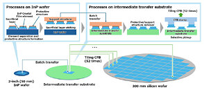
OKI has successfully developed Tiling crystal film bonding (CFB) technology using its proprietary CFB technology. This technology makes possible the heterogeneous integration of small-diameter optical semiconductor wafers onto 300 mm silicon wafers, heretofore not possible due to wafer size restrictions, and will contribute to the advancement of rapidly growing photonics-electronics convergence technology. OKI aims to achieve early commercialization through collaboration with partner companies and universities.
Rapid advances in artificial intelligence (AI) in recent years has fueled growing demand for data centers, making it a serious social issue to suppress increases in power consumption while expanding data processing capabilities. One solution to such a challenge currently drawing attention is technologies that achieve high-density, high-speed transmission, and low power consumption, applying photonics-electronics convergence technology that combines electronic and optical circuits. In particular, the heterogeneous integration of optical semiconductors onto silicon wafers is expected to improve performance still further by enabling the integration of silicon photonics with optical semiconductors.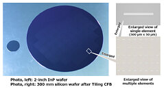
Read full story
More...


